
Laser & Photonics Components
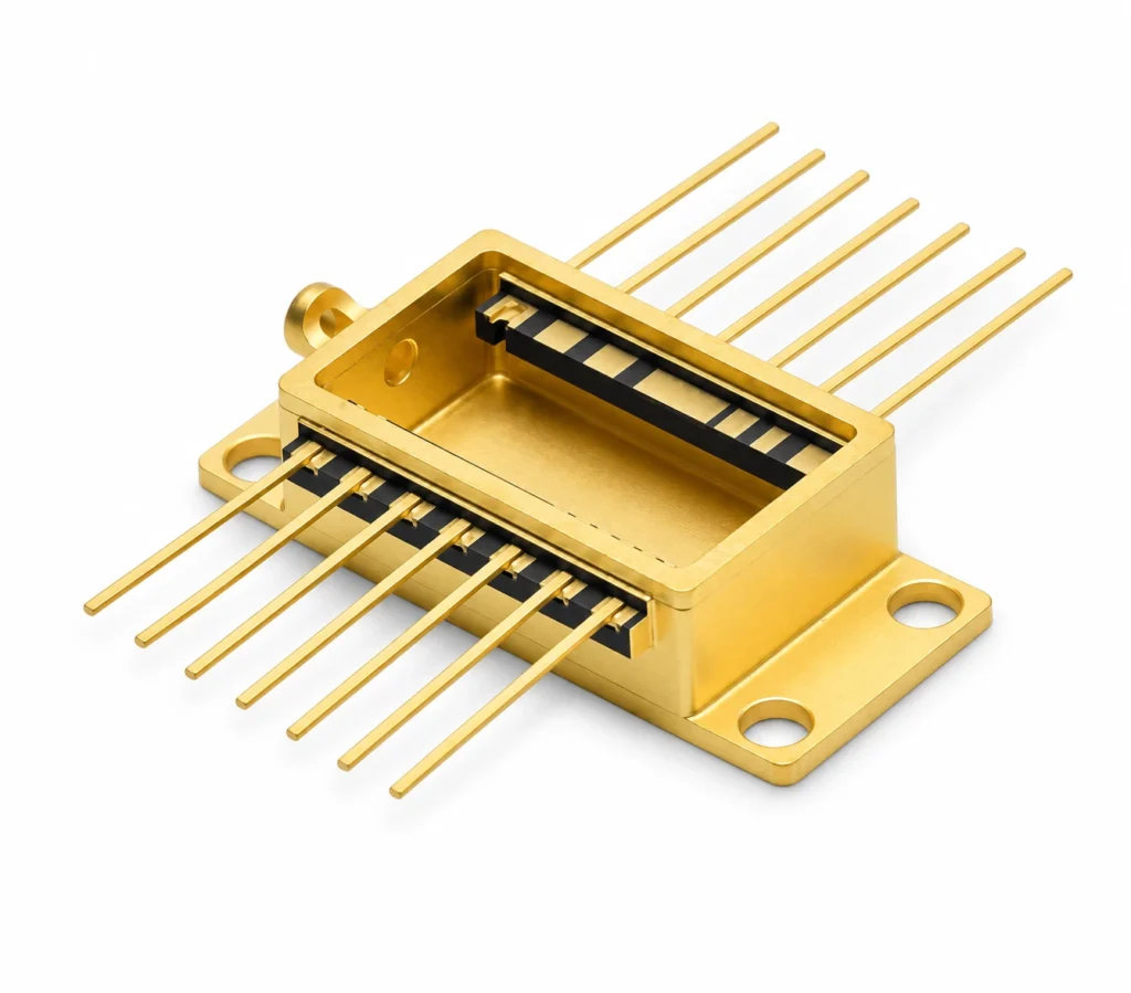
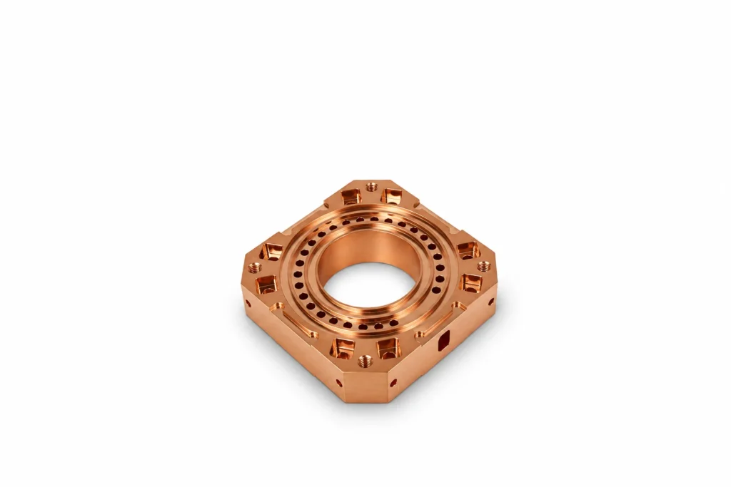
Custom A-QCW Annular Laser Diode Stack Package Housing
Precision-machined annular housing for A-QCW laser diode bar stacks used for side-pumping rod-shaped gain media. Housing only, to customer drawings.
ExploreTry a part name, a material (Kovar, SUS304) or a process (CNC turning, anodizing). Press Enter for full results.
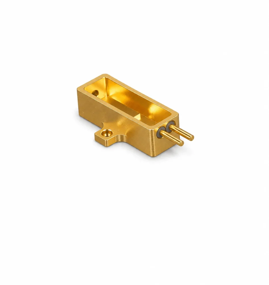
Custom precision-machined TO-style package housing for power semiconductor and optoelectronic devices.
Design considerations
Technical specifications
| Parameter | Value | Unit / Note |
|---|---|---|
| Product type | Custom TO Package Housing | |
| Material options | Kovar / stainless steel / copper alloys and other approved metals | Design review; not interchangeable by default |
| Critical features | TO-style body, terminal interfaces and cavity or lid interface | |
| Finish | Gold / nickel / selective plating; thickness and coverage per drawing | |
| Dimensions and tolerances | Per approved drawing | Reviewed for material, geometry and process |
| Inspection | Dimensions and visual condition; CMM for applicable features | Methods and reports agreed per project |
Values shown are per this product entry; customer drawings take precedence.
Manufacturing
Applications
Custom housings for power semiconductor devices, TO-style electronic packages, power switching and control modules, laser/optoelectronic assemblies and other applications requiring metal package bodies and electrical feedthrough interfaces. Final suitability depends on customer design.
Provide the drawing revision, 2D drawing and STEP model, quantity, material grade, requirements for to-style body, terminal interfaces and cavity or lid interface, coating areas and thickness, and acceptance criteria. Photographs show custom variants, not a standard size or pin count.
Insulation, leak tightness, vacuum suitability, electrical ratings and thermal performance require design-specific verification under agreed conditions; appearance or material alone does not establish them.
FAQ
Provide the drawing revision, 2D drawing and STEP model, quantity, material grade, requirements for to-style body, terminal interfaces and cavity or lid interface, coating areas and thickness, and acceptance criteria. Photographs show custom variants, not a standard size or pin count.
TO-style body, terminal interfaces and cavity or lid interface; dimensions, tolerances and process compatibility are confirmed during engineering review.
No. Tolerances depend on the drawing, material and geometry. Insulation, leak tightness, vacuum suitability, electrical ratings and thermal performance require design-specific verification under agreed conditions; appearance or material alone does not establish them.
More in this family
Laser & Photonics Components
Precision-machined annular housing for A-QCW laser diode bar stacks used for side-pumping rod-shaped gain media. Housing only, to customer drawings.
ExploreLaser & Photonics Components
Jingyixin manufactures custom high-precision ceramic-to-metal package housings for electronic, optoelectronic and sensor assemblies.
ExploreLaser & Photonics Components
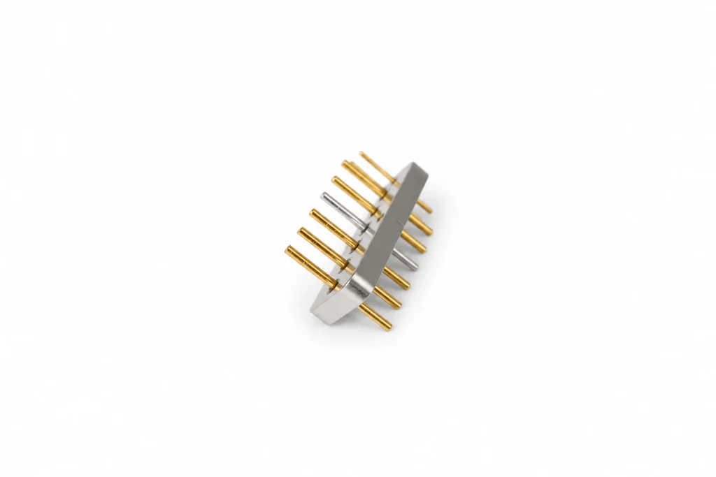
Jingyixin manufactures custom high-precision dual-row multi-pin electrical feedthrough assemblies for electrical interconnection in optoelectronic packages, laser systems, semiconductor equipment and industrial instruments.
ExploreRequest a Quote
Share your drawing, material, quantity and critical requirements for a manufacturing review.